School had picked up soon after publishing Part 1 of this project, in which I built the first working prototype. With the semester winding down, I figured now was a good time to continue. In this segment, we’ll create a custom PCB for our previous prototype, then model and print a new enclosure for it. I’m also hoping to tailor a custom voltage divider solution for the rather stiff FSR sensors we previously used. Let’s see how far we can get here.
Electrical CAD
Schematic
As you can see from the following schematic, we’ve condensed this little organ system in a more organized way, which is helpful when designing the PCB layout. Our circuitry consists of an input, data processing, audio processing, auditory output, visual output, and BMS (Battery Management System) section.

PCB Layout
For the layout, I first had to make a decision regarding the number of layers our board would consist of. While researching the fundamentals of PCB design, I came across Rick Hartley’s lecture on How to Achieve Proper Grounding, which explains many techniques in a highly concentrated way. Here are a few key takeaways I put into deciding between two and four layers:
- We want to prevent the return paths, i.e. “grounds” for this circuit, from interfering with one another.
- Digital signals are generally considered high-frequency (MHz to GHz range), while analog signals are considered slow or low-frequency (Hz to MHz range). “Slow” and “fast” are relative.
- We have both signal types serving a variety of functions. For instance, the SGTL5000 audio codec is functioning as a DAC (Digital to Analog Converter), translating the digital I2S protocol’s audio data from the Teensy 4.1 into an analog signal for our PAM8302A amplifier. And that’s just one of our signal paths.
- Long traces can act like antennas, warping adjacent signals resulting in mayhem.
I chose to go with a 4-layer board. This will not only save us space in terms of routing, but also (hopefully) improve our signal’s integrity by reducing noise and crosstalk — both subsets of EMI (Electromagnetic interference). There are many other variables at play here that my current understanding doesn’t allow me to perceive, but I see this project as a learning opportunity, so let’s move!
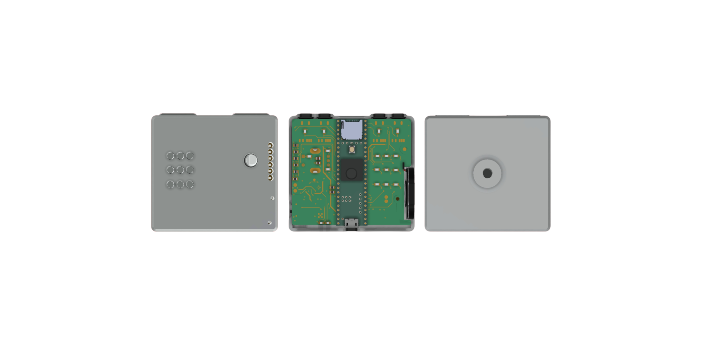
Since I’ve been advised to avoid auto-routers, I got to work laying out the traces, and here’s what I came up with:


Satisfied with the board stackup and routing, I put in an order at JLCPCB, and shifted my attention to the enclosure design.
Mechanical CAD
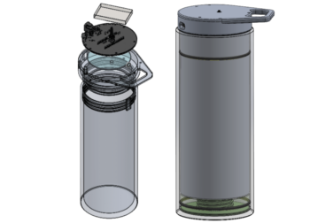
Enclosure
If you recall from Part 1 of this project, my original goal was to give this device a “glove” form factor. That said, I felt it wasn’t quite time to work with fabrics or e-textiles yet, because we’re still just laying a foundation to be built upon. After modeling a few designs, I settled on one that doesn’t quite fit the “glove” profile, but it will sit distal to the wrist joint:

You can take a look inside in the 3D browser here if you’d like, and the .stl files will be on my GitHub soon. While a short mounting height will be needed, this feels preferable to the bulky wristwatch prototype we had before.

This fulfills the “…sketch out my ideas without imposing on other activities…” portion of our user story to a greater extent. We’re not quite there yet, but at least its moving in the right direction.
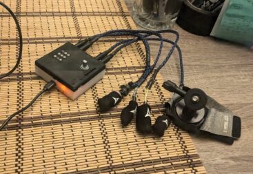
PCB Assembly (Attempt #1)
SMD Soldering
The printed circuit boards arrived two weeks later from JLCPCB, and the soldering began. In order to debug any potential issues, I chose to start with the active and passive 0805 components of the power section first. A little bit of heat and a lot of flux later, and here’s the result of that portion:

At this point I soldered in my 350 mAh lipo battery, flipped the switch on, and…

Assessing Blockers
The image above doesn’t do what happened next much justice, but the TPS61090 IC actually began to smoke, and I hate to be a party-killer, but I am running low on time. Thankfully, this is a personal project, so a post-mortem assessment and corresponding fix will patiently wait until my next post.
There is one clue I’ll close with that will serve as the starting point next time:
See those two lights above? The red LED is attached to the collector of a PNP bipolar junction transistor (BJT), which is ultimately driven by the LBO (Low-Battery Output) pin of the TPS61090 boosting IC. The blue LED is driven by the +5V output pins of the TPS61090 as well. When I flipped the DPDT (Double Pole, Double Throw) switch, the ENable pin on the step-up converter pulled to GND, effectively shutting everything off from our load. The blue LED shut off, but for some reason the red LBO LED stayed on. The smoke emitting from the boost converter points to a short circuit. There may be a solder bridge, contact failure, or a design error. Regardless, it’ll be a prime opportunity to learn about the internal circuitry of the charge and boost ICs!