It’s been a busy season, but winter break has opened my schedule up to tackle this project. Previously in Part 2, I designed a PCB that incorporated a LiPo battery charging and boost conversion circuit to power a 5V microcontroller and downstream components. We left off with an alarming sizzle as the boost converter IC fried, so below, I’ll identify what happened, fix it, and complete this project.

A. Power Troubleshooting
I. Revisiting a Clue

Clue: Moments before its incineration, the TPS61090 was supposed to respond to the switch I flipped by turning off a BJT and subsequent red LED, but that didn’t happen. The first thing I realized was that I needed to look closer at this transistor (T1):
The PNP transistor (T1) acts as a switch controlled by the LBO (12) pin (the output of the battery comparator). Its base is connected to LBO, and its emitter receives current from the upstream output of the MCP73871 charge controller. LBO is placed in a floating, high-impedance (Hi-Z) state when the battery voltage is above 3.2V, as is also the case when the TPS61090 is in “Shutdown” mode. The latter of those two cases results from the EN (11) pin being connected to GND via finger switch. When the battery EMF drops below 3.2V, a connected voltage divider feeding the LBI (9) pin (the input of the battery comparator) delivers a proportional voltage drop below the LBI’s 500 mV threshold logic, which in turn drives the LBO pin active low. This causes the voltage at the base of the PNP transistor to drop, creating a positive-to-negative voltage potential difference from its emitter to its base. In this state, the PNP transistor is on, and the base-emitter junction is said to be “forward-biased.”
In this forward-biased state, the transistor allows current to flow from the upstream emitter to the downstream collector, through a 1 kΩ resistor, and into the anode of the red LED. The LED emits light as current flows, and its cathode connects to GND, completing the circuit.

With my memory jogged, I revisited the physical layout of the boost converter pins. I realized that smoke likely arose due to a short circuit between the LBO and EN pins. If this were true, then LBO could be forced into an active low state when EN is connected to GND, thereby forward-biasing the transistor and lighting the red LED (Undesired). Flipping the switch pulls EN high, but then the LBI pin becomes active, and if the battery is below 3.2V, it drives the LBO pin into an active low state, and illuminates the red LED (Desired). This unexpected condition likely created excessive current flow through the shorted path, resulting in the thermal damage we observed.
So, where there’s smoke, there’s fire I guess. But here’s the real kicker…
When I sat down to test for this short, however, there was no continuity between the two pins. I took a brief break while browsing an electrical forum, and saw a mention of someone mistakenly using water-soluble plumbing flux. To that, I raised my eyebrows and went back to check whether I might have done the same. Sure enough, I’d been using an improper flux compound to wet all my solder joints. In doing so, I likely destroyed most of that board in a savage bout of corrosion. Frankly, I’m amazed the current made it all the way to our step-up converter.
So this time around, I’m going to start with a fresh board, populate the power delivery section, and troubleshoot any (hopefully) smaller issues that arise. And I’m excited, because hey, that’s an important skill to have when designing a product!
Also, just to reiterate that point on proper flux usage, here’s the sort of nastiness plumbing flux can inflict on electronics, and a visual clarification on what I will NOT be using:


II. Power Overview

Zooming out to provide some context on our power flow, I am switching between a 5V USB and a 3.7V-4.2 V Lipo battery supply. Charging and power delivery is the bottom-right portion highlighted below (Yellow), where the micro USB port feeds USB power at 5V to the Teensy’s VUSB pin (#1), which passes this to an MCP73871 charge controller (U2, #2). Directly below this are two terminals indicated by the ellipse (Orange) where the battery joins the circuit. Both power sources then feed into the TPS61090 boost converter (U1, #3). On battery power, the discharged voltage will be stepped up to 5V here. Finally, power is delivered back into the Teensy microcontroller through the +5V “VIN” pin (#4).

Note: Sorry about the mirror image. This ^ image is flipped horizontally when compared to most orientations in this post.
III. MCP73871 Charge Controller
The MCP73871 has proven capable of robust power-path management in several battery and solar-powered projects I’ve read about, provided it’s configured correctly. Below are details on several behaviors I troubleshot.
a. PROG1 Pin & Charge Rate

The image above shows the original 1.0 kΩ resistor I put in series from PROG1 to GND, which I decided to refit with a 3.3 kΩ resistor to yield a ~0.87C charge rate for our 350 mAh LiPo (about 303 mA).
Measuring the through-hole resistor I used shows the actual resistance is around 2.86 kΩ, bringing the charge current closer to ~350 mA (roughly 1C). While within spec, this slightly higher rate could heat up the battery by potentially prolonging the constant voltage (CV) phase, the third and final stage of MCP73871’s charging cycle. Because of this, I sourced a 3.3 kΩ resistor with tighter tolerances for future iterations on this board.
b. PROG3 Pin & Termination Threshold

Above you’ll see the original 100 kΩ resistor I had chosen to set our charge termination threshold to 10 mA. I wanted to raise this threshold, so I added a second 100 kΩ resistor in parallel at the PROG3 pin to achieve 50 kΩ. This sets the termination current to around 20 mA, which is adequate for a 350 mAh cell. Minor variations in this threshold (plus or minus 5 to 10 mA) are probably normal, but I want this as specific as possible, so I also sourced a 50 kΩ SMD resistor for future iterations.
$$
R_{\text{eq}} = \frac{1000 V}{\left(\frac{1}{R_1} + \frac{1}{R_2}\right)} = \frac{1000 V}{\left(\frac{1}{100\,\text{k}\Omega} + \frac{1}{100\,\text{k}\Omega}\right)} = 50\,\text{k}\Omega
$$
While doing this, I learned that those reciprocal resistances in the denominator are equivalent to units of conductivity called Mhos (℧), which I believe are also called Siemens (S) in the standard SI system. Wiring resistors in parallel like this physically provide more paths for our current to flow, reducing net resistance, like cars in a busy city having more routes to take home.
Here’s the math you need if you’d like to program your own charge termination threshold on the MCP73871, and an example of the modifications I made to the PROG3 (And PROG1) net:
EQUATION 4-2 of this datasheet:
$$
I_{\text{TERMINATION}} = \frac{1000 \, V}{R_{\text{PROG3}}}
$$
Where:
\begin{align*}
R_{\text{PROG3}} & = \text{kilo-ohms (k}\Omega\text{)} \\
I_{\text{TERMINATION}} & = \text{milliampere (mA)}
\end{align*}
Tip: For two identical resistors in parallel, take your identical value, and divide by two:
$$
R_{\text{eq}} = \frac{R}{2} = \frac{100\,\text{k}\Omega}{2} = 50\,\text{k}\Omega
$$
And here are my janky modifications with the PROG3 (Upper) and PROG1 (Lower) through-hole resistors:

c. STAT2 Pin (From Green LED) Reliability

Occasionally the green LED (Connected to STAT2 pin through a 1 kΩ resistor) won’t illuminate after 4+ hours of charging. I isolated this problem to the STAT2 pin for two reasons. One, the battery would consistently level off to 4.21 V when charging. Two, I broke the circuit open to measure the current flowing into the battery and got 18 mA. In other words, the charging feature wasn’t the issue here. In theory, the STAT2 pin is supposed to transition from a high impedance (Hi-Z) state to a low state once the constant voltage phase of the charging cycle terminates, indicating a “charge complete” status of our battery, and lighting the green LED.

Possible Causes & Related Behavior:
- Solder/Flux Issue (Most likely)
- Despite reworking these pins using proper rosin-based flux, a second coat of solder, and 90% isopropyl alcohol to clean the joints, there’s still a chance that the STAT2 pin (or some related pin) isn’t making a fully reliable connection.
- Doing a “dye and pry” test would be nice if I could spare another board and the time involved, because it would confirm or rule out hidden micro-gaps as our cause. However, that falls beyond the scope of this project’s troubleshooting.
- USB-Cable “Bump” Phenomenon
- When the battery is above 4.19 V, physically jostling the USB-A end of different cables sometimes illuminates the green LED and shuts off the orange one. The MCP73871 may be re-checking the battery voltage and “realizing” that it’s already reached the termination threshold we’d set with the PROG3 resistor, causing STAT2 to finally switch low, which would explain this behavior.
- Noise or Overshadowed Termination Conditions
- Parasitic currents, contact resistance, or slightly off-kilter charge parameters may mask or delay the microcontroller’s recognition of a fully charged battery. For instance, if the system load is drawing marginal current, the termination logic might take longer to register a low enough current to trigger “charge complete.”
Note: I’ve encountered several faulty solder joints while troubleshooting, and I’m fairly certain that this is the culprit here, but I can’t seem to reach the part of the QFN pad that needs to be reworked with my soldering iron. Since there is no overheating after lengthy charge sessions, and since all other behavior is now normal, I’m going to keep an eye on this and eventually populate a future board in a reflow oven. Afterward, I’ll test STAT2’s functionality specifically and report back to this red text.
IV. TPS61090 Boost Converter
Meanwhile, the TPS61090 synchronous boost converter handles stepping up the 3.7 V nominal LiPo to the 5 V supply for the microcontroller:
a. Leakage Voltage at VOUT Pin
- Finding: When EN is grounded to disable the TPS61090, VOUT doesn’t drop instantly to 0 V. It briefly hovers around ~0.24 V, then gradually falls closer to 0 V.
- Cause: Residual charge on the output capacitor and minor leakage currents. I read that this is normal. Within a minute or so, the output capacitors discharge through the load and/or internal paths.
b. Screeching Inductor Noise

- Past Issue: Before applying a second round of solder, the inductor would emit a high-pitched whine when (A) the battery was topped off at 4.21 V, and (B) the charger was supplying power via the upstream USB port.
- Resolution: Changing the MCP73871’s programming resistor values and resoldering its QFN leads ensured a stable input supply to the TPS61090, and this seems to be how I got rid of the inductor screech.
c. Confirming Downstream Load Stability
- Teensy 4.1 Microcontroller: Observed no unusual resets or brownouts. With EN disabled, only a negligible leftover voltage remains at the load, which soon dissipates.
- No Adverse Effects: The minor residual voltage doesn’t appear to harm the system.
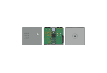
V. Complete PCB Assembly
After troubleshooting the power circuit, I populated the board with the remaining components, doing each sub circuit systematically, and testing for proper functionality between soldering. Some of the button’s corresponding indicator LEDs are a still a bit bright, so I may swap out the resistors later.

B. Mechanical Enclosure Revision
I spent an evening in SolidWorks redesigning what had started as a Fusion360 sketch and getting the dimensions right to best secure the PCB. A week after submitting the STL files to my local library for printing, the prints came in, and I was pleasantly surpised by both the functionality and the aesthetics of the upper nylon enclosure, the lower PETG enclosure, as well as the PETG button actuators. I placed a print in queue for a set of each material with the intent of using the better result, but they both worked fine, so we’re going Neapolitan ice cream. I’m was also pleasantly surprised that this simple captive button design held so well while allowing for the vertical movement we needed.


C. Software Development & Integration
With the enclosure assembled, I shifted focus to software development to ensure proper interaction between the microcontroller, MIDI interface, and onboard peripherals. Below are key developments and refinements in the firmware.
I. MIDI Handling & Sequencer Logic
The core of this drum machine is a real-time MIDI event handler that captures FSR (force-sensitive resistor) triggers, translates them into velocity-sensitive MIDI notes, and sequences them for playback.
- MIDI Event Processing
- Implemented a robust MIDIHandler class to manage incoming FSR inputs and translate them into MIDI Note On/Off messages. Each event is timestamped and written to a MIDI file on the SD card for looped playback.
- Sequencer Logic
- The SequencerHandler ensures that notes are triggered in sync with the internal clock, preserving groove timing across multiple layers of sequences.
- FSR Velocity Sensing
- Using ResponsiveAnalogRead, I fine-tuned FSR input responsiveness, eliminating debounce noise and improving velocity accuracy for dynamic drumming.
II. SD-Based Sample Playback & Flash Storage
Beyond MIDI sequencing, I implemented SD card sample browsing and SerialFlash playback for triggering custom drum samples.
- Live Sample Assignment
- Pressing an FSR while in “Browse Mode” assigns the currently selected sample from the SD card to that pad, dynamically storing it in onboard flash memory.
- Real-Time Flash Playback
- Once stored, samples are retrieved from flash memory for low-latency playback via AudioPlaySerialflashRaw. This allows seamless layering of custom drum sounds with MIDI sequencing.
- Sample Preview & Selection
- Implemented a non-blocking preview system that lets users audition samples in real-time before assigning them to an FSR pad.
III. Clocking & Sync Behavior
To maintain accurate loop timing and synchronization with external devices:
- Internal Clock Generation
- A steady MIDI clock signal is generated when “Internal Clock Mode” is active, ensuring precise loop playback timing.
- External Clock Input
- Added logic for external clock sync, allowing the drum machine to stay in time with an external MIDI source or analog clock pulse.
- Adaptive Tempo Scaling
- Adjusted note times dynamically when tempo changes occur mid-sequence to preserve groove integrity.
IV. UI & Control Enhancements
A few usability improvements were made:
- LED Feedback & Indicators
- Integrated LED states to visually indicate recording, sequence playback, and mute status.
- Undo & Track Mute Functionality
- Implemented an “Undo” button to clear the last recorded sequence and track mute toggling to isolate layers during playback.
- Metronome Toggle
- Added a metronome feature with adjustable tempo for timing reference.
Project Conclusion
With the fundamental PCB, enclosure, and software framework in place and functional, I’ve decided to close this project for the time being. In retrospect, I’m almost satisfied with how this turned out, and here is a demo to round things off.